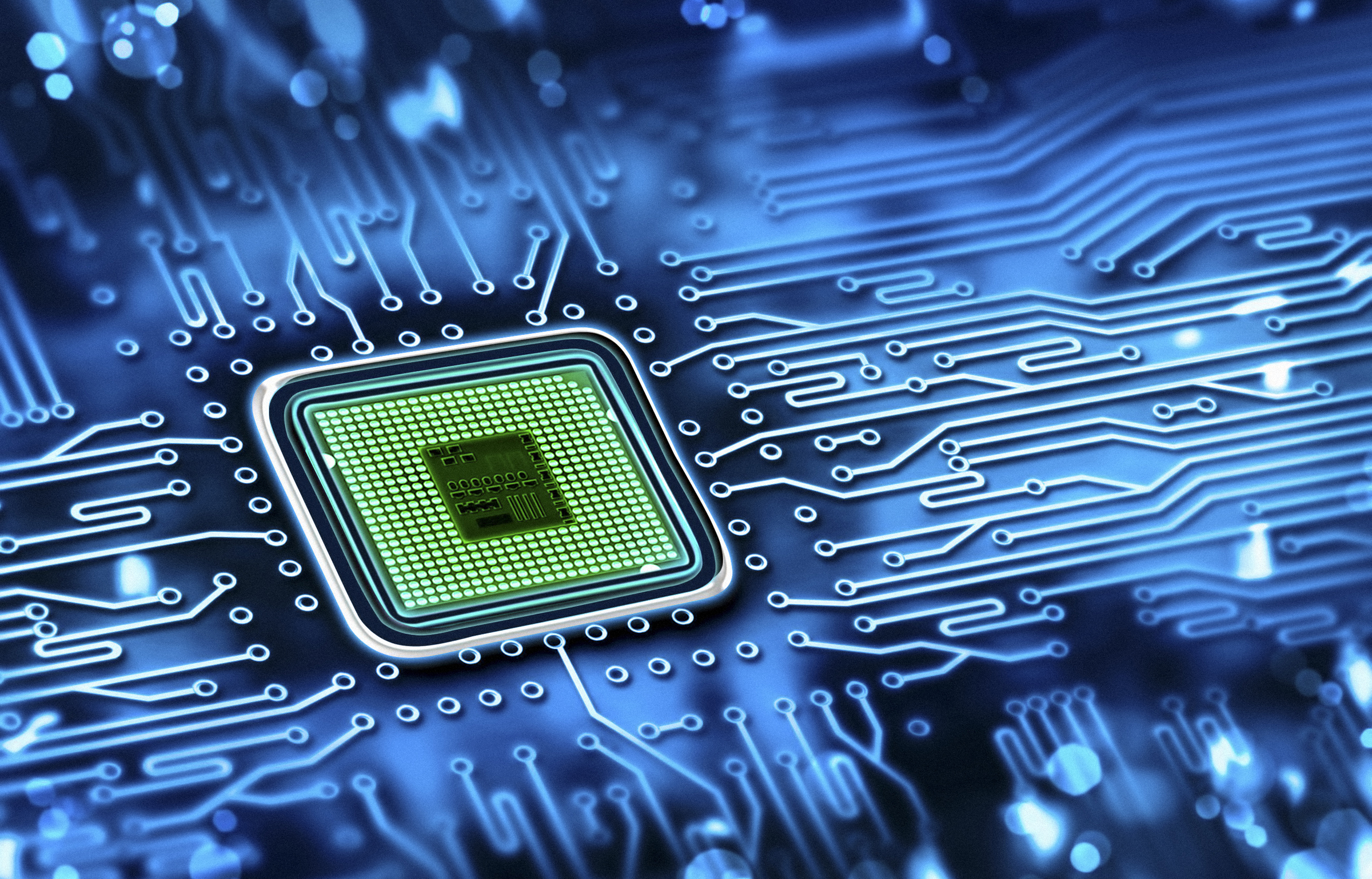
computer chip
- November 09, 2017
NEW White Paper Available!
Gallagher Fluid Seals recently added a new white paper to its Resources Page, Perfluoroelastomers for the Semiconductor Industry, written by Russ Schnell. Below is an excerpt from the new white paper discussing plasma process manufacturing. You can download the white paper in its entirety by clicking on the thumbnail to the right.
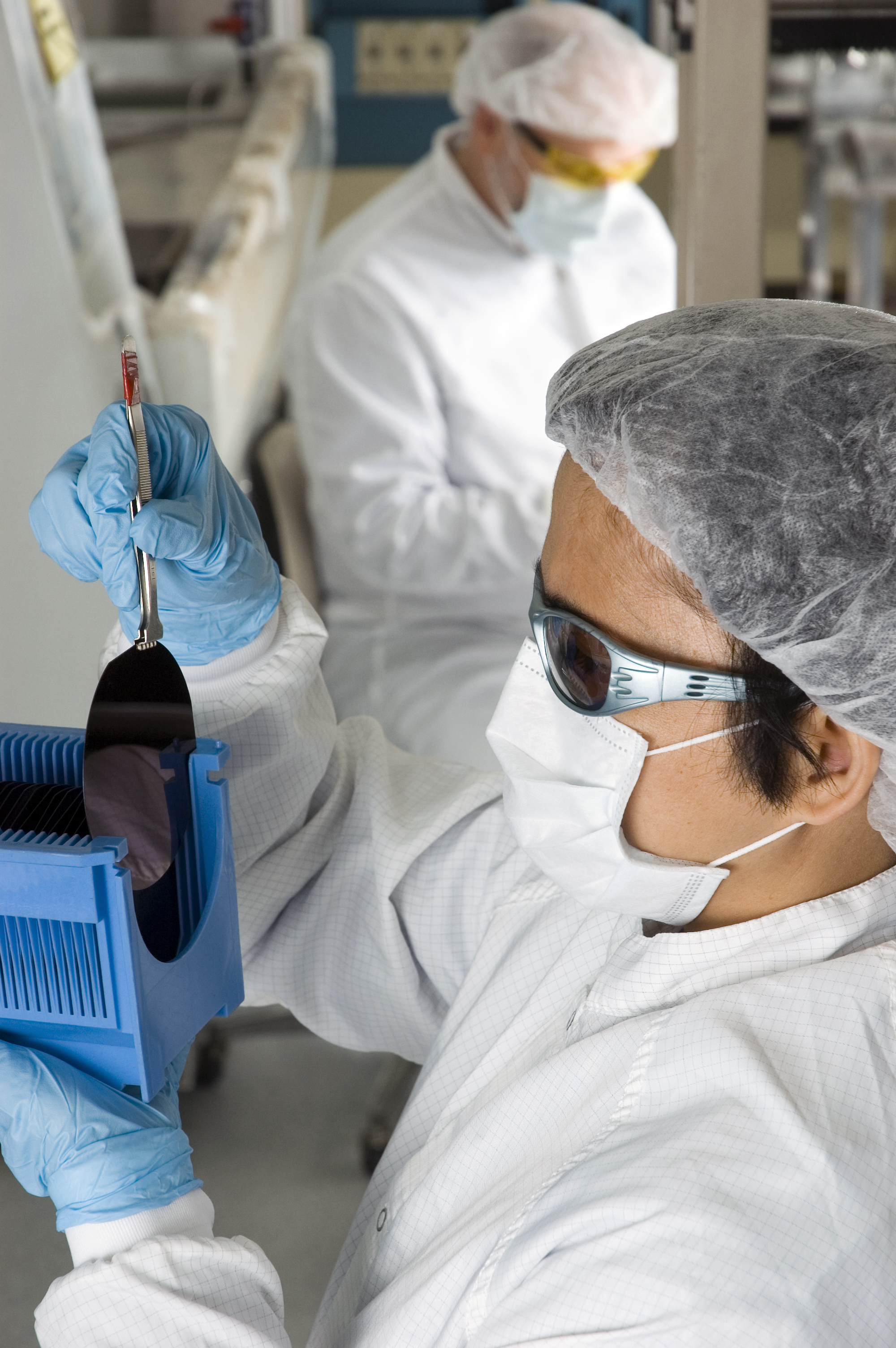
Although this is a smaller segment of the semiconductor chip manufacturing industry, it still plays an important role. Wet processes can be used in cleaning, etching, and other steps in chip manufacture. Wafers may be cleaned and rinsed after initial wafer preparation. This step removes residual particles and other contamination on the wafer surface. The wafer may then be exposed to chemicals for adhesion promotion and/or photoresist deposition. After photoresist is applied to the wafer surface, the wafer can be exposed to a number of photolithography steps. The wafer may then be exposed to liquid developer solutions and photoresist stripping solutions. Resist strippers usually involve aggressive acids or organic solvents. Finally, wet processes can also be used in etching processes, which typically involve strong acids.
- September 12, 2017
NEW White Paper Available!
Gallagher Fluid Seals has added a new white paper to its Resources Page, Perfluoroelastomers for the Semiconductor Industry, written by Russ Schnell. Below is an excerpt from the new white paper. You can download it in its entirety by clicking on the thumbnail to the right.
The semiconductor industry, one of today’s major industries, produces integrated circuits (chips) which have found their way into everyday devices from toasters to smartphones to high speed computers. Integrated circuits are expected to perform operations faster and faster while attaining ever higher levels of reliability. As these chips become more complex and powerful the process for their manufacture becomes more complicated. Years ago a chip may have gone through 100 steps as underlying circuits were constructed. Now chips may go through more than 400 steps and the complexity of these circuits, and their capability, has greatly increased. This also results in more opportunities for problems during manufacture. Line widths, the width of the electrical pathways, have decreased in order to pack more capacity into each chip. This dictates that contaminants from the production equipment, gas streams, seals, etc., must be essentially eliminated to avoid contamination and chip malfunction.