semicon
- February 06, 2018
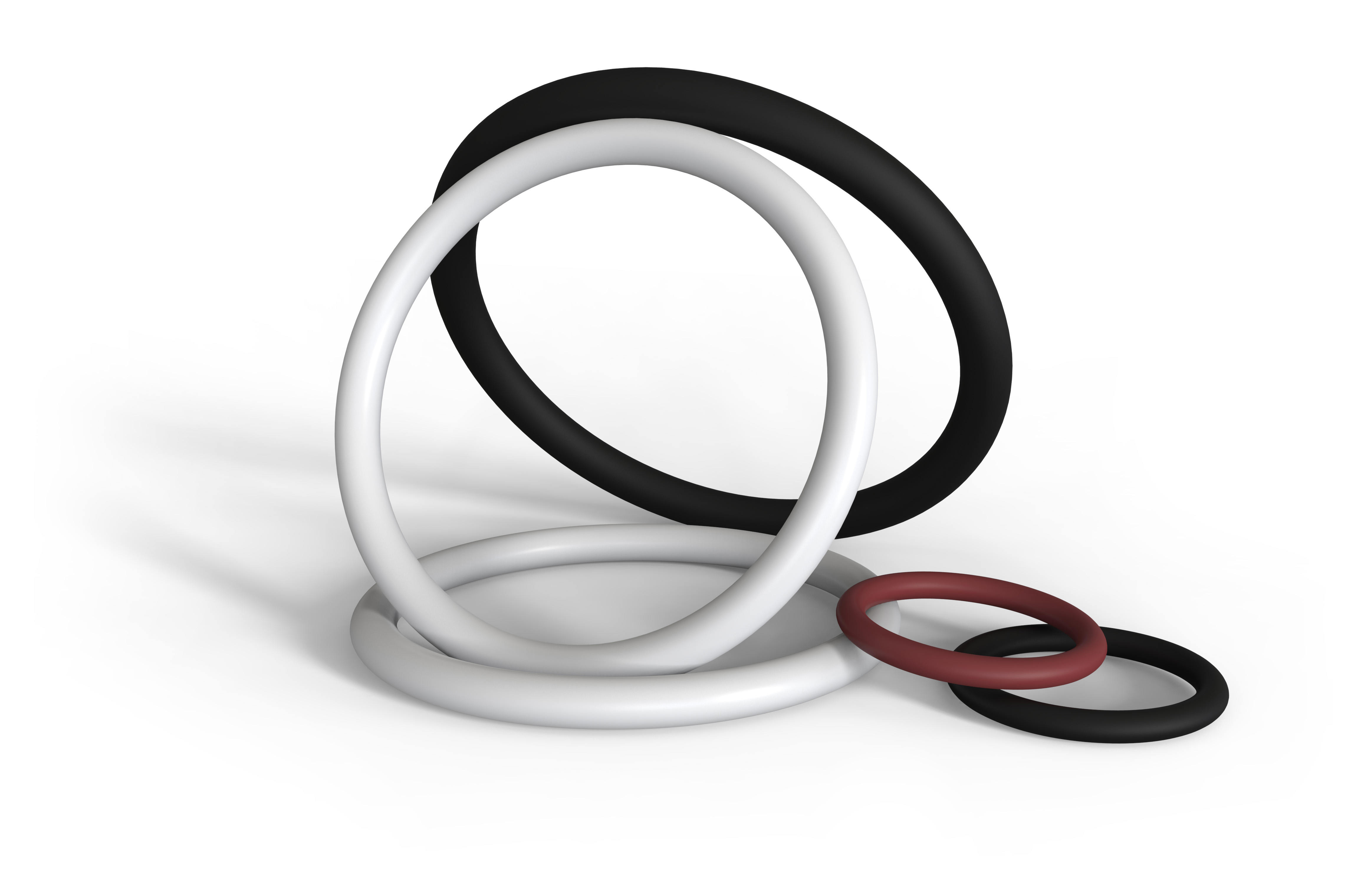
Gallagher recently published its Failure Modes of Elastomers in the Semiconductor Industry White Paper, now available for download on our site. This white paper discusses common issues that occur with elastomer seals in the semiconductor industry. The excerpt below is the first section of our new white paper, discussing groove design and seal leakage. To download the entire white paper, visit our Resources Page, or click on the image to the right.
Failure Modes for Elastomers in the Semiconductor Industry
High performance elastomers are found in many applications in the semiconductor industry (see paper titled Perfluoroelastomers in the Semiconductor Industry). Though perfluoroelastomer (FFKM) seals are formulated to meet the highest performance requirements of integrated circuit (chip) manufacturers, even these elastomers can’t solve every sealing application nor will they last forever in service. Additionally, end users need to understand subtle performance differences between perfluoroelastomers in the same product line. For example, one product may be better at minimizing particle generation while another may be better for high temperature services.
- November 28, 2017
NEW White Paper Available!
Gallagher Fluid Seals recently added a new white paper to its Resources Page, Perfluoroelastomers for the Semiconductor Industry, written by Russ Schnell. Below is an excerpt from the new white paper discussing the key reasons to choose perfluoroelastomers over fluoroelastomers for semiconductor manufacturing. You can download the white paper in its entirety by clicking on the thumbnail to the right.
Perfluoroelastomers (e.g. Kalrez® parts), often replace fluoroelastomer (e.g. Viton®) in semiconductor applications. However, even though perfluoroelastomers are the highest performance elastomers, there are still subtle differences between products. It is suggested that the elastomer supplier be contacted regarding the optimum product and seal design for specific applications. As mentioned above the key characteristics of perfluoroelastomers include:
- Lower offgassing than other elastomers, especially at temperatures above 200°C, which lowers the risk of product contamination.
- Better sealing force retention (lower compression set) at temperatures over 200°C, which is critical for longer service.
Best overall chemical resistance of any elastomer family. - Formulations with extremely low particle generation in aggressive process environments.
- Generally higher gas permeation than fluoroelastomers.
- Higher coefficient of thermal expansion when compared to fluoroelastomers. Proper seal design will account for this and optimize performance.
- November 09, 2017
NEW White Paper Available!
Gallagher Fluid Seals recently added a new white paper to its Resources Page, Perfluoroelastomers for the Semiconductor Industry, written by Russ Schnell. Below is an excerpt from the new white paper discussing plasma process manufacturing. You can download the white paper in its entirety by clicking on the thumbnail to the right.
Although this is a smaller segment of the semiconductor chip manufacturing industry, it still plays an important role. Wet processes can be used in cleaning, etching, and other steps in chip manufacture. Wafers may be cleaned and rinsed after initial wafer preparation. This step removes residual particles and other contamination on the wafer surface. The wafer may then be exposed to chemicals for adhesion promotion and/or photoresist deposition. After photoresist is applied to the wafer surface, the wafer can be exposed to a number of photolithography steps. The wafer may then be exposed to liquid developer solutions and photoresist stripping solutions. Resist strippers usually involve aggressive acids or organic solvents. Finally, wet processes can also be used in etching processes, which typically involve strong acids.
- October 03, 2017
NEW White Paper Available!
Gallagher Fluid Seals recently added a new white paper to its Resources Page, Perfluoroelastomers for the Semiconductor Industry, written by Russ Schnell. Below is an excerpt from the new white paper discussing plasma process manufacturing. You can download the white paper in its entirety by clicking on the thumbnail to the right.
Plasma Process
In plasma process manufacturing, a remote plasma source generates a plasma gas. Note that this type of process is run in a vacuum environment. This gas is composed of ions, electrons, radicals and neutral particles. The flow of these particles must be carefully controlled for etching, deposition, or ashing/stripping processes. These processes often use oxygen, fluorine, and other exotic plasma gases, which are extremely aggressive to many materials. In addition, cleaning processes often use oxygen plasma. Precise control of the plasma gas in the chamber is critical so processes perform as expected, for all the individual chips, across the entire diameter of the wafer.
In the plasma process, which typically operate under a high vacuum, FFKM seals can be critical for maintaining system integrity and providing a long seal life. The term “long seal life” is relative. However these seals must perform at high temperatures, up to 250°C, and still maintain low offgassing and low particle generation to prevent contaminating the manufacturing process. In some cases, under extremely aggressive conditions of plasma gases and high temperatures, 6-8 weeks may be considered a long service life for an elastomer seal.
- September 19, 2017
NEW White Paper Available!
Gallagher Fluid Seals recently added a new white paper to its Resources Page, Perfluoroelastomers for the Semiconductor Industry, written by Russ Schnell. Below is an excerpt from the new white paper. You can download it in its entirety by clicking on the thumbnail to the right.
The following is a simplified process chart for chip manufacture in the semiconductor industry:
Following the process shown above:
- A silicon wafer has been prepared from an ingot by cutting and polishing. The wafer then has layers of material applied. These include a silicon oxide layer, a silicon nitride layer and a layer of photoresist.
- A light is then projected through a reticle and a lens unto the wafer surface. This pattern is projected numerous times onto the wafer for each chip.
- September 12, 2017
NEW White Paper Available!
Gallagher Fluid Seals has added a new white paper to its Resources Page, Perfluoroelastomers for the Semiconductor Industry, written by Russ Schnell. Below is an excerpt from the new white paper. You can download it in its entirety by clicking on the thumbnail to the right.
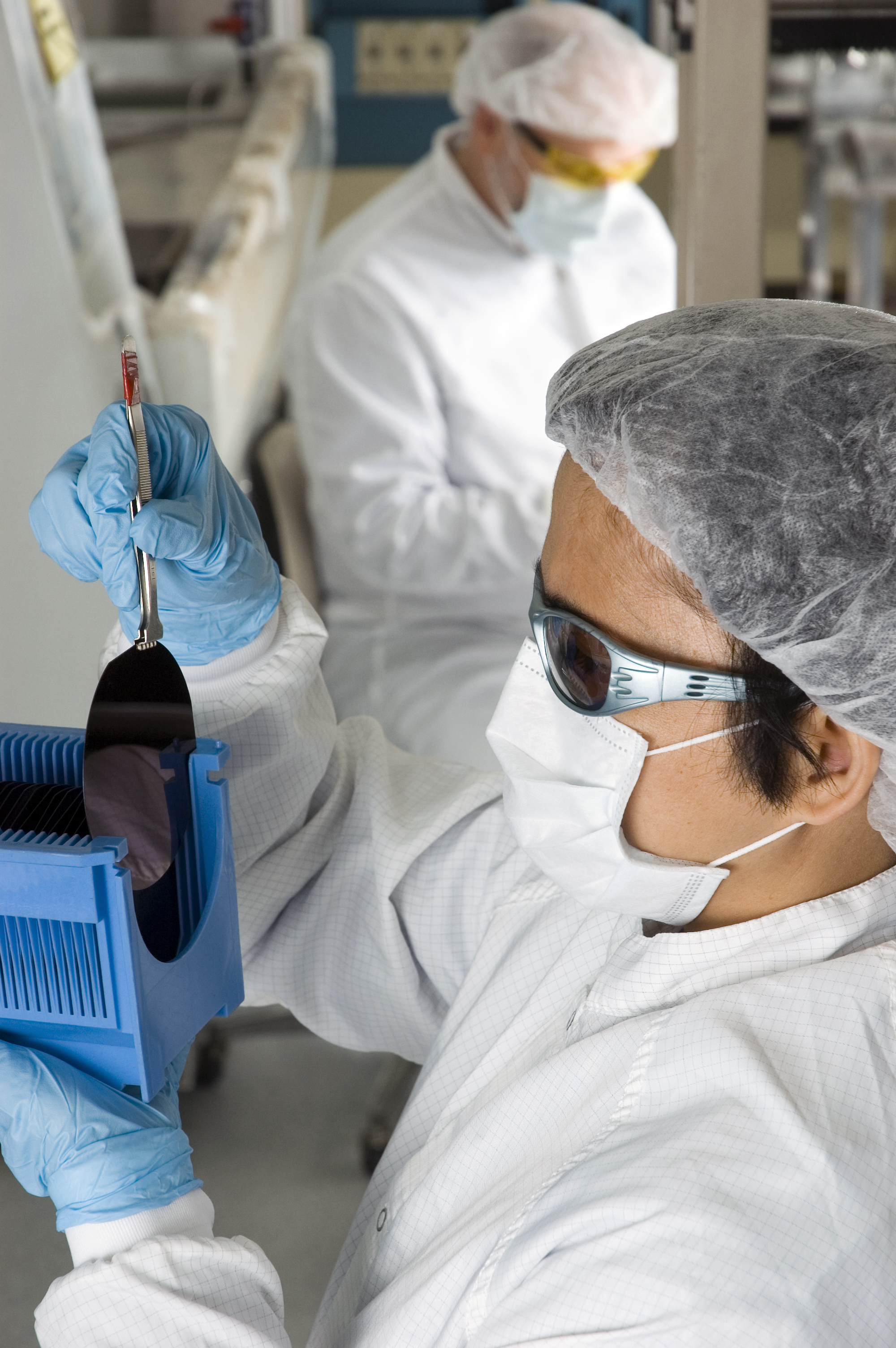
The semiconductor industry, one of today’s major industries, produces integrated circuits (chips) which have found their way into everyday devices from toasters to smartphones to high speed computers. Integrated circuits are expected to perform operations faster and faster while attaining ever higher levels of reliability. As these chips become more complex and powerful the process for their manufacture becomes more complicated. Years ago a chip may have gone through 100 steps as underlying circuits were constructed. Now chips may go through more than 400 steps and the complexity of these circuits, and their capability, has greatly increased. This also results in more opportunities for problems during manufacture. Line widths, the width of the electrical pathways, have decreased in order to pack more capacity into each chip. This dictates that contaminants from the production equipment, gas streams, seals, etc., must be essentially eliminated to avoid contamination and chip malfunction.