thermal process
- October 17, 2017
NEW White Paper Available!
Gallagher Fluid Seals recently added a new white paper to its Resources Page, Perfluoroelastomers for the Semiconductor Industry, written by Russ Schnell. Below is an excerpt from the new white paper discussing thermal process manufacturing. You can download the white paper in its entirety by clicking on the thumbnail to the right.
The term “thermal process” covers a fairly wide range of applications. Per the name, these application temperatures are generally higher than plasma processes, ranging up to 300°C. This general term can cover processes including: Sub Atmospheric Chemical Vapor Deposition (SACVD), Metal CVD, Low Pressure CVD (LPCVD), Rapid Thermal Processing (RTP), and Oxidation or Diffusion furnaces. In these applications the wafers and the equipment that surrounds them, are heated to extremely high temperatures. In the case of thermal deposition, the high temperatures aid in the uniformity of the coating thickness.
Rapid Thermal Processing is used to very rapidly heat a wafer up to temperatures of 1000°C or greater for short periods of time. “Rapid Thermal Processing (RTP) can be used to reduce the thermal redistribution of impurities at high temperature…. RTP was originally developed for ion implant anneal, but has broadened its application to oxide growth, chemical vapor deposition, and silicidation.” For oxidation or diffusion furnaces, the applications are different, but still involve high temperatures. For oxidation applications, the procedure involves formation of a thin oxide film on the wafer surface. For diffusion applications, the furnace may assist in silicon dioxide formation on the wafer surface or it may be used to diffuse dopants in the wafer. For these applications, temperatures may range up to 1200°C.
- September 19, 2017
NEW White Paper Available!
Gallagher Fluid Seals recently added a new white paper to its Resources Page, Perfluoroelastomers for the Semiconductor Industry, written by Russ Schnell. Below is an excerpt from the new white paper. You can download it in its entirety by clicking on the thumbnail to the right.
The following is a simplified process chart for chip manufacture in the semiconductor industry:
Following the process shown above:
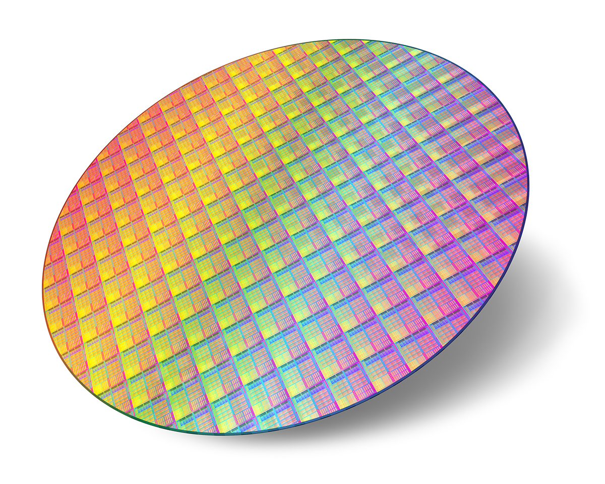
- A silicon wafer has been prepared from an ingot by cutting and polishing. The wafer then has layers of material applied. These include a silicon oxide layer, a silicon nitride layer and a layer of photoresist.
- A light is then projected through a reticle and a lens unto the wafer surface. This pattern is projected numerous times onto the wafer for each chip.