Semiconductor
- March 09, 2026
Thermal Solutions for Tight Semiconductor Cavities
Today’s tech landscape is rapidly evolving, especially in the automotive and communications sectors. Driven by the increased adoption of 5G and 6G as well as advances in data processing, data speeds, and internet connectivity, all sorts of applications from medical devices to EV car batteries are getting faster, more efficient, and more connected.
To keep up with the demand and shifting requirements, manufacturers are now commonly developing
- December 23, 2025
Kalrez® Bonded Door Seals
Bonded door seals for gate valves and slit valve door seal applications provide improved sealing performance versus conventional O-rings by reducing particle generation, extending seal life, and minimizing replacement time during preventive maintenance.
DuPont™ Kalrez® bonded door seals are designed for easy installation and low particle generation. They combine a custom seal design and proprietary
- October 27, 2025
White Paper Available!
Check out our Resources Page for dozens of free downloadable content, including Perfluoroelastomers for the Semiconductor Industry, written by Russ Schnell. Below is an excerpt from the white paper discussing thermal process manufacturing. Learn more and download this white paper by following the link below.
The term “thermal process” covers a fairly wide range of applications. Per the name, these application temperatures are generally higher than plasma processes, ranging up to 300°C. This general term can cover processes including: Sub Atmospheric Chemical Vapor Deposition (SACVD), Metal CVD, Low Pressure CVD (LPCVD), Rapid Thermal Processing (RTP), and Oxidation or Diffusion furnaces. In these applications the wafers and the equipment that surrounds them, are heated to extremely high temperatures. In the case of thermal deposition, the high temperatures aid in the uniformity of the coating thickness.
Rapid Thermal Processing is used to very rapidly heat a wafer up to temperatures of 1000°C or greater for short periods of time. “Rapid Thermal Processing (RTP) can be used to reduce the thermal redistribution of impurities at high temperature…. RTP was originally developed for ion implant anneal, but has broadened its application to oxide growth, chemical vapor deposition, and silicidation.” For oxidation or diffusion furnaces, the applications are different, but still involve high temperatures. For oxidation applications, the procedure involves formation of a thin oxide film on the wafer surface. For diffusion applications, the furnace may assist in silicon dioxide formation on the wafer surface or it may be used to diffuse dopants in the wafer. For these applications, temperatures may range up to 1200°C.
- October 02, 2018
Article re-posted with permission from Parker Hannifin Sealing & Shielding Team.
Original content can be found on Parker’s Blog.
Semiconductor FFKM Offers Low Particle Generation AND Extreme Etch Resistance
In the world of semiconductor manufacturing, performance requirements are driving circuit sizes smaller and smaller, causing increased sensitivity to wafer defects. In parallel, the number of manufacturing steps has also increased driving a need for improved tool utilization and leaving more opportunity for these defects to be introduced. Identifying and eliminating the sources of defects is a tedious but necessary process to improve wafer yield.
What impact does seal contamination make?
One very distinct source of defects are the seals within a fab’s tool. Plasmas involved in both deposition, etch and cleaning processes utilize aggressive chemistries that put even high-functioning perfluorinated sealing compounds to the test. Much room for improvement has been left in this industry with many seal materials still posing significant threats to defectivity or downtime despite being designed for low particle generation or etch resistance.
How can Parker ULTRA™ change the industry?
Parker’s UltraTM FF302 Perfluorelastomer has proven success in CVD and etch applications, putting this material at the top of its class. Typically, seal materials for semiconductor applications are optimized for low particulation or extreme etch resistance, however, Ultra FF302 provides both attributes in one material. Laboratory testing shows Ultra FF302 has lower erosion in aggressive plasma chemistries even when compared to today’s leading elastomeric materials (Figure 1 below shows comparison erosion levels of various etch resistant perfluoroelastmers after exposure to O2 plasma).
- November 28, 2017
NEW White Paper Available!
Gallagher Fluid Seals recently added a new white paper to its Resources Page, Perfluoroelastomers for the Semiconductor Industry, written by Russ Schnell. Below is an excerpt from the new white paper discussing the key reasons to choose perfluoroelastomers over fluoroelastomers for semiconductor manufacturing. You can download the white paper in its entirety by clicking on the thumbnail to the right.
Perfluoroelastomers (e.g. Kalrez® parts), often replace fluoroelastomer (e.g. Viton®) in semiconductor applications. However, even though perfluoroelastomers are the highest performance elastomers, there are still subtle differences between products. It is suggested that the elastomer supplier be contacted regarding the optimum product and seal design for specific applications. As mentioned above the key characteristics of perfluoroelastomers include:
- Lower offgassing than other elastomers, especially at temperatures above 200°C, which lowers the risk of product contamination.
- Better sealing force retention (lower compression set) at temperatures over 200°C, which is critical for longer service.
Best overall chemical resistance of any elastomer family. - Formulations with extremely low particle generation in aggressive process environments.
- Generally higher gas permeation than fluoroelastomers.
- Higher coefficient of thermal expansion when compared to fluoroelastomers. Proper seal design will account for this and optimize performance.
- November 09, 2017
NEW White Paper Available!
Gallagher Fluid Seals recently added a new white paper to its Resources Page, Perfluoroelastomers for the Semiconductor Industry, written by Russ Schnell. Below is an excerpt from the new white paper discussing plasma process manufacturing. You can download the white paper in its entirety by clicking on the thumbnail to the right.
Although this is a smaller segment of the semiconductor chip manufacturing industry, it still plays an important role. Wet processes can be used in cleaning, etching, and other steps in chip manufacture. Wafers may be cleaned and rinsed after initial wafer preparation. This step removes residual particles and other contamination on the wafer surface. The wafer may then be exposed to chemicals for adhesion promotion and/or photoresist deposition. After photoresist is applied to the wafer surface, the wafer can be exposed to a number of photolithography steps. The wafer may then be exposed to liquid developer solutions and photoresist stripping solutions. Resist strippers usually involve aggressive acids or organic solvents. Finally, wet processes can also be used in etching processes, which typically involve strong acids.
- October 03, 2017
NEW White Paper Available!
Gallagher Fluid Seals recently added a new white paper to its Resources Page, Perfluoroelastomers for the Semiconductor Industry, written by Russ Schnell. Below is an excerpt from the new white paper discussing plasma process manufacturing. You can download the white paper in its entirety by clicking on the thumbnail to the right.
Plasma Process
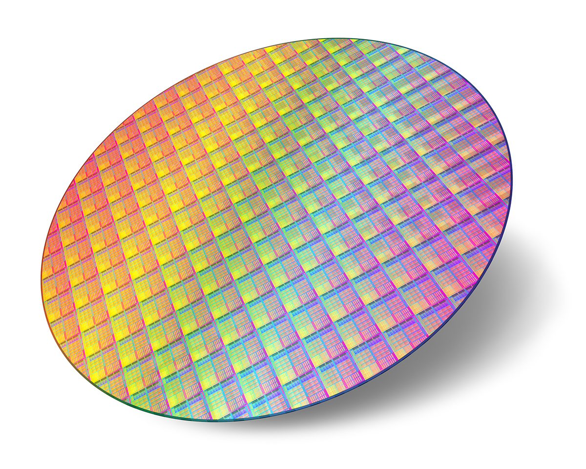
In plasma process manufacturing, a remote plasma source generates a plasma gas. Note that this type of process is run in a vacuum environment. This gas is composed of ions, electrons, radicals and neutral particles. The flow of these particles must be carefully controlled for etching, deposition, or ashing/stripping processes. These processes often use oxygen, fluorine, and other exotic plasma gases, which are extremely aggressive to many materials. In addition, cleaning processes often use oxygen plasma. Precise control of the plasma gas in the chamber is critical so processes perform as expected, for all the individual chips, across the entire diameter of the wafer.
In the plasma process, which typically operate under a high vacuum, FFKM seals can be critical for maintaining system integrity and providing a long seal life. The term “long seal life” is relative. However these seals must perform at high temperatures, up to 250°C, and still maintain low offgassing and low particle generation to prevent contaminating the manufacturing process. In some cases, under extremely aggressive conditions of plasma gases and high temperatures, 6-8 weeks may be considered a long service life for an elastomer seal.
- September 19, 2017
NEW White Paper Available!
Gallagher Fluid Seals recently added a new white paper to its Resources Page, Perfluoroelastomers for the Semiconductor Industry, written by Russ Schnell. Below is an excerpt from the new white paper. You can download it in its entirety by clicking on the thumbnail to the right.
The following is a simplified process chart for chip manufacture in the semiconductor industry:
Following the process shown above:
- A silicon wafer has been prepared from an ingot by cutting and polishing. The wafer then has layers of material applied. These include a silicon oxide layer, a silicon nitride layer and a layer of photoresist.
- A light is then projected through a reticle and a lens unto the wafer surface. This pattern is projected numerous times onto the wafer for each chip.


